MENU
CLOSE
3 Ways Application-Optimized PLLs & DLLs
Help Optimize SoC Performance
by Mo Faisal, President & CEO, Movellus
I. Overview
Phase-locked loops (PLLs) and delay-locked loops (DLLs) provide critical clocking functions in today’s chips. When properly optimized for the specific SoC, these circuits improve the entire chip’s power, performance, and area.
Such optimization for the exact application has become critically important in all markets from high-performance cloud computing to ultra-low power Edge AI and IoT.
This paper presents how Application Optimized™ IP is helping the industry move toward extreme customization of silicon and covers three specific ways optimization for the end application enhances performance and reduces power and area (PPA).

Timing circuits such as PLLs & DLLs are essential in every market
Application-Optimized IP are IP blocks that are customized to exact customer specifications and their specific application requirements using 100% digital, fully synthesizable IP technology – delivered in weeks without impacting the tapeout schedule.
Three key benefits of digital Application-Optimized IP are:
- Performance scales with process nodes.
- Faster time-to-market due to full synthesizability.
- Extreme PPA efficiency. (e.g. 700-nanowatt PLL with 100X smaller area already in production.)
The discussion in this paper focuses on PLLs & DLLs; it is important to note that each factor discussed also applies to other analog functions, such as ADCs and DACs. Below are a few key factors behind the industry’s drive toward highly customized, application-specific SoCs.
II. Industry’s Drive to Application-Specific SoCs
Over the last decade, the demand for custom silicon specifically optimized for end user applications as well as data has increased significantly. For example, Apple, Samsung and more recently Tesla have demonstrated the advantages of co-optimizing silicon and software.
Additionally, the need for customization has been recognized by adjacent players such as equipment and materials companies. One example of this is the META center launched by Applied Materials in 2019 to facilitate customization of the entire development stack from materials to systems for greater efficiency.
Moreover, foundries have responded to this need for customization by introducing multiple flavors of each process tuned for different market segments, e.g. IoT, mobile and high-performance compute. Large semiconductor companies often have the wafer volume to justify their own custom process adjustments suited to their application.
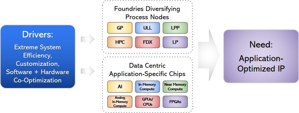
Industry’s drive toward extreme customization creates need for application-optimized IP
This drive towards extreme customization has put significant pressure on the analog IP ecosystem both from PPA and time-to-market perspectives. Even though PLLs and DLLs have been an essential part of chips for decades, it is only recently that 100% digital, synthesizable technology has become available to address the need for extreme customization.
When not optimized, critical analog functions such as PLLs & DLLs could adversely impact the power and performance of the entire system. The rest of this discussion provides reasons Application-optimized synthesizable PLLs & DLLs instead of off-the-shelf custom analog PLLs & DLLs are becoming the de facto choice for customized chips.
III. Three Ways Application-Optimized PLLs/DLLs Help Optimize SoC Performance
Before discussing the three reasons that make Application-Optimized synthesizable PLLs/DLLs the enabling innovation for chip level performance optimization, below are a few ways that settling for either off-the-shelf IP or in-house custom development of IP can adversely impact your ability to optimize your chip.
- When purchasing off-the-shelf analog IP, you end up customizing your chip for the IP rather than customizing the IP for your SoC and the desired application. You may be required to adjust your chip’s layout or DFT plan as well as the power delivery network to fit the IP into your chip.
- IP availability can often dictate the decision to choose a certain process node. Companies often find themselves settling for older process nodes in the interest of IP availability and this adversely impacts the power and performance of the entire system. Settling for an older process can make the entire system less competitive.
- Chip design teams could opt to develop their own analog IP in house. However, this significantly extends the duration of the design cycle and adds risk to meeting the target market window.
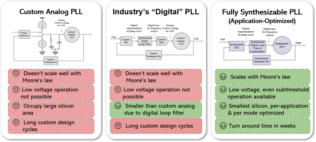
Custom Analog vs. “Digital” vs. Fully Synthesizable PLLs
In the subsections below, we compare 100% digital, synthesized PLLs & DLLs to their analog counterparts in terms of capability to achieve optimal chip-level PPA. Important factors such as power, performance, operating voltage, and time-to-market are discussed below in a digital vs. analog format. Each subsection illustrates the impact on the chip-level performance as well.
1. Low Supply Voltage Operation Results in Reduced Chip Power
Many of today’s electronic devices are battery operated with stringent power requirements. These strict power requirements often necessitate low supply voltage operation which is a challenge for analog circuits.
Digital circuit architectures do not require precise voltage/current biasing which gives digital PLLs and DLLs higher flexibility in supporting the lower supply voltage associated with low power designs.
The relationship between power and supply voltage is quadratic. Therefore, supply voltage is a strong knob for power reduction. Designers can lower supply voltages to reduce power consumption in more energy constrained applications or scenarios and raise it when faster operation is needed.
Analog circuits require most transistors to remain in the saturation region which puts a stringent lower limit on the supply voltage. The need for higher supply voltages not only affects the power of the SoC, but also the BOM for the entire system as it may require additional power management ICs in the system.
Certain low voltage operations, such as near-threshold, may not even be possible with analog for high volume production with sufficient robustness. Additionally, analog circuits are very sensitive to noise in low-voltage operation while digital circuits have a much higher level of noise immunity.
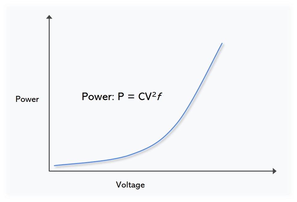
Power vs. Supply voltage
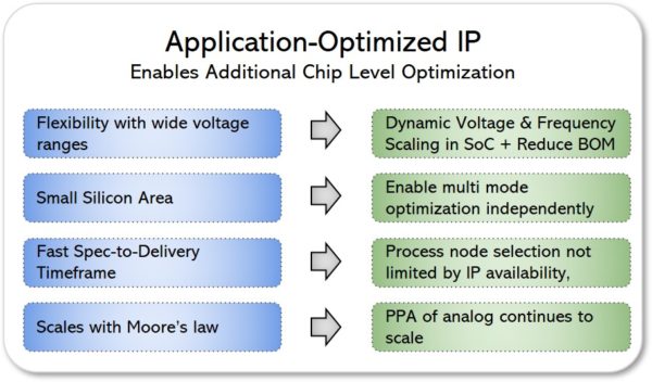
Impact: Supply voltage flexibility and ability to reduce chip power consumption. The flexibility to operate at a wide range of supply voltages enables design teams to reduce the power consumption of the entire chip instead of adding additional complexity to the power delivery network.
Eliminating the need for higher supply voltages can also reduce the overall system-level cost by simplifying board-level power management.
2. Silicon Area
Area is always a major concern for high volume applications.
Digital. Depending on the application, all digital PLLs and DLLs can be many times smaller than their analog IP counterparts. This is because they are not dependent on matching and passive elements that are required for analog implementations. Matching and passive elements are a dominant contributor to the area of custom analog IP blocks.
The smaller size for digital IP provides a chip-level power advantage because SoC architects have greater flexibility. Given the smaller area, they can utilize multiple PLLs, with each PLL tuned to better fit the chip’s specific modes, such as standby and sleep, rather than using one general purpose analog IP.
Analog. Analog and mixed analog/digital PLLs have inherently larger area because they require matching and passive elements that increase their size. This is particularly true for slower, low frequency chips (e.g. IoT/edge) because the size of the passive elements is inversely proportional to the frequency of operation.
Impact: Ability to individually optimize SoC operating modes without area or schedule penalties. Modern SoCs commonly rely on sleep and standby modes to further reduce the power consumption of the system by tuning the performance of the chip according to the workload. Adding a separate low-area standby-optimized PLL for applications that have long sleep cycles can save overall power consumption.
This is highly beneficial for devices such as mobile phones, where users do not have constant interactions with all the various functions. Applications are opened on demand by touch or through voice interaction. With off-the-shelf IP, chip design teams end up settling for high power mission mode IP even for power-sensitive sleep and standby modes.
3. Faster Specification-to-Delivery Timeframe
Digital circuits have enjoyed unprecedented automation over the years making it possible to go from RTL to GDS in a matter of hours. This, however, does not apply to analog design.
Digital. 100% digital, synthesizable PLLs/DLLs offer the following benefits:
- Advanced process nodes always use digital lead vehicles to prove out their manufacturing capability. Analog circuits typically lag because they take much longer to develop. At any given point in time, digital circuits are much more time-tested and proven in comparison to their analog counterparts.
- Completely digital architectures enable rapid RTL-to-GDS implementation and optimization by taking full advantage of the speed of logic synthesis and place and route technology that is not available for custom analog.
- The master RTL code base can be configured and reconfigured to generate RTL code that will precisely meet each customer’s specs.
- Because digital implementations can be efficiently ported between processes in a matter of weeks, the IP can readily take full advantage of the power and performance opportunities provided by the more advanced nodes or adjustments in customer architecture.
Analog. It is well understood that custom analog blocks can take many months to deliver. For advanced process nodes, the design time required may even be measured in years.
Impact: Ability to select optimal process node and enhance chip optimization. Analog IP availability is an important factor that can drive chip design teams to settle for older nodes and therefore pay both a power and performance penalty.
The quick turn-around of synthesizable PLLs & DLLs can enable chip design teams to select the best process node for their application without worrying about the analog IP availability. It also enables you to ensure your IP is optimally customized for your chip to deliver the best possible performance, power, and area.
IV. Conclusion
Application-Optimized PLLs & DLLs that are fully synthesizable serve as a key enabler for optimal SoC clock distribution networks as they directly impact the power, area, performance, and cost of the entire system.
ABOUT MOVELLUS
Movellus’ technology has been silicon-proven in multiple fabs and process nodes since 2015 and has been in volume production since 2018.
ABOUT THE AUTHOR

Dr. Mo Faisal, Founder, President & CEO, Movellus
As Movellus CEO, Mo Faisal is responsible for the company’s overall strategic direction and execution. Prior to founding Movellus, Dr. Faisal held positions at semiconductor companies such as Intel and PMC Sierra.
Faisal received his B.S. from the University of Waterloo, and his M.S. and Ph.D. from the University of Michigan and holds several patents. Dr. Faisal was named a “Top 20 Entrepreneur” by the University of Michigan Zell Lurie Institute.
Stay Connected
Stay Connected
By clicking “Accept”, you consent to the use of ALL the cookies. ACCEPTREJECT
Privacy Overview
| Cookie | Duration | Description |
|---|---|---|
| __hssrc | session | This cookie is set by Hubspot whenever it changes the session cookie. The __hssrc cookie set to 1 indicates that the user has restarted the browser, and if the cookie does not exist, it is assumed to be a new session. |
| cookielawinfo-checbox-analytics | 11 months | This cookie is set by GDPR Cookie Consent plugin. The cookie is used to store the user consent for the cookies in the category "Analytics". |
| cookielawinfo-checbox-functional | 11 months | The cookie is set by GDPR cookie consent to record the user consent for the cookies in the category "Functional". |
| cookielawinfo-checbox-others | 11 months | This cookie is set by GDPR Cookie Consent plugin. The cookie is used to store the user consent for the cookies in the category "Other. |
| cookielawinfo-checkbox-advertisement | 1 year | Set by the GDPR Cookie Consent plugin, this cookie is used to record the user consent for the cookies in the "Advertisement" category . |
| cookielawinfo-checkbox-necessary | 11 months | This cookie is set by GDPR Cookie Consent plugin. The cookies is used to store the user consent for the cookies in the category "Necessary". |
| cookielawinfo-checkbox-performance | 11 months | This cookie is set by GDPR Cookie Consent plugin. The cookie is used to store the user consent for the cookies in the category "Performance". |
| CookieLawInfoConsent | 1 year | Records the default button state of the corresponding category & the status of CCPA. It works only in coordination with the primary cookie. |
| JSESSIONID | session | The JSESSIONID cookie is used by New Relic to store a session identifier so that New Relic can monitor session counts for an application. |
| viewed_cookie_policy | 11 months | The cookie is set by the GDPR Cookie Consent plugin and is used to store whether or not user has consented to the use of cookies. It does not store any personal data. |
| Cookie | Duration | Description |
|---|---|---|
| __cf_bm | 30 minutes | This cookie, set by Cloudflare, is used to support Cloudflare Bot Management. |
| Cookie | Duration | Description |
|---|---|---|
| __hssc | session | HubSpot sets this cookie to keep track of sessions and to determine if HubSpot should increment the session number and timestamps in the __hstc cookie. |
| __hstc | session | This is the main cookie set by Hubspot, for tracking visitors. It contains the domain, initial timestamp (first visit), last timestamp (last visit), current timestamp (this visit), and session number (increments for each subsequent session). |
| _ga | 2 years | The _ga cookie, installed by Google Analytics, calculates visitor, session and campaign data and also keeps track of site usage for the site's analytics report. The cookie stores information anonymously and assigns a randomly generated number to recognize unique visitors. |
| _ga_F75FB76KBW | 2 years | This cookie is installed by Google Analytics. |
| _gat_gtag_UA_60322432_1 | 1 minute | Set by Google to distinguish users. |
| _gid | 1 day | Installed by Google Analytics, _gid cookie stores information on how visitors use a website, while also creating an analytics report of the website's performance. Some of the data that are collected include the number of visitors, their source, and the pages they visit anonymously. |
| hubspotutk | session | HubSpot sets this cookie to keep track of the visitors to the website. This cookie is passed to HubSpot on form submission and used when deduplicating contacts. |